SiC is revolutionising EV/HEV power electronics, but is the packaging up to the job?
Add bookmarkAs the automotive industry moves towards “Zero Emissions” transportation, manufacturers are rapidly ramping up their electrification programs; with most OEMs targeting 2025 for significant volumes of Battery Electric (BEVs) and Hybrid Electric Vehicles (HEVs).
To meet customer expectations on range, charge-time and performance these EVs require power electronic devices capable of efficient and effective operation at elevated temperatures. Hence, power modules are being developed using Wide Band-gap (WBG) silicon carbide (SiC) and gallium nitride (GaN) technologies.
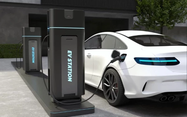
Image Source: Charged EVs
SiC set become the de facto EV/ HEV semiconductor technology
These WBG semiconductors hold great promise to significantly outperform and eventually replace traditional Si components that are typically capable of handling band-gap energy (Eg) of about 1.1eV. While there are R&D efforts into various WBG semiconductors - including diamond, aluminum nitride, and gallium oxide - SiC with an Eg of 3.3eV and GaN at 3.4eV have currently reached a level of maturity that has seen the technologies rapidly gaining ground over Si for demanding applications, such as traction Power Electronics (PE) in EVs and HEVs.
For example, where silicon has a breakdown electric field of 0.3 MV/cm, SiC can withstand up to 2.8 MV/cm, and its internal resistance is 100 times smaller than that of silicon. As a result, applications can handle the same level of current using a smaller chip resulting in smaller systems.
Today, SiC technology’s added value is widely understood and accepted by the power electronics community. Yole’s analysts peg CAGR at 28% through 2022.
Importantly for EVs/ HEVs, compared to Si, SiC-based power devices can operate at higher temperatures with higher thermal conductivity, higher breakdown voltage at lower on-stage resistance, faster switching speed, lower conduction and switching on-state loss, with exceptional radiation hardness.
Consequently, SiC inverters allow for smaller cooling solutions and greater thermal-management design flexibility due to significantly less heat generation. As a result, SiC inverters deliver a four-fold increase in drive frequency over conventional technology in step-up converter applications, while unlocking significant improvements in power output and density by allowing for smaller and lighter peripheral components.
However, in demanding EV/ HEV power electronics applications, performance doesn’t only rely on innovations in high-voltage main circuits and high-performance control circuits, it requires constant improvements in the structural design technology used to mount these components in a compact package while enabling reliable and durable systems that are resistant to vibration and heat.
Working toward an improved WBG future
While SiC and GaN devices have demonstrated higher efficiency than Si-based devices in PE applications, reliability concerns still limit the market penetration of WBG technologies. As WBG technologies mature, without strategies to establish their reliability, the PE community will not gain confidence in their use.
Gaining a better understanding of degradation/failure mechanisms under harsh conditions (i.e., stresses such as high voltages and/or high temperatures) is key to designing more robust WBG components.
In 2017, JEDEC a global leader in developing open standards for the microelectronics industry, formed the JC-70 committee on “Wide Band-gap Power Electronic Conversion Semiconductors.”
Focusing on Reliability and Qualification Procedures, Datasheet Elements and Parameters, and Test and Characterization Methods, the team hopes to create the mature industry infrastructure needed to design reliable and cost-effective power supplies. Led by interim chairs from Infineon, Texas Instruments, and Wolfspeed, the new JC-70 committee will initially have two subcommittees formed around Gallium Nitride and Silicon Carbide.
Companies push the boundaries of packaging and improve reliability
As one of the interim chairs of the JC-70 committee, Wolfspeed, a Cree Company and a leader in silicon carbide (SiC) power products, has developed a 900V, 10mΩ MOSFET rated for 196 A of continuous drain current at a case temperature of 25°C. The device enables the reduction of EV drive-train inverter losses by 78 percent based on EPA combined city/highway mileage standards.
This efficiency improvement offers designers new options in terms of range, battery usage, packaging and vehicle design, while ensuring reliability through lower thermal stress.
However, in addition to reducing the cost and optimizing performance of SiC devices, the PE community needs to identify and address technical issues at all levels of design, manufacturing, packaging, and qualification that currently constrain WBG power components.
Key module and packaging challenges include the need to improve high voltage insulation, thermal management, partial discharge, and EMI to enable high-performance modules (e.g., double-sided cooled power modules operating at higher junction temperatures of between 175oC to 200oC), and high-performance discrete packages that can operate at higher temperatures and voltages.
An important component, often not discussed in packaging terms is the substrate used in PE modules.
The substrate represents the backbone of power electronic modules as it carries the active component – the semiconductor die.
As such it:
• Insulates the heatsink and inverter housing
• Provides the topological interconnections
• Dissipates the heat generated by the semiconductors
Due to the wide ranging requirements of PE modules, different types of anorganic ceramic materials are used.
Compared to organic insulation materials, which are widely used for logic and microelectronic circuits, these ceramic materials provide outstanding properties like:
• Excellent thermal conductivity
• Very good electrical insulation properties
• Thermal coefficient of expansion close to semiconductor materials
Moreover, with most of the heat being generated by the high-voltage main circuit of the inverter in HEVs and EVs, improving cooling of these components is key to reducing inverter size and weight. Most suppliers, such as Hitachi Automotive Systems have achieved major reductions in inverter size and mass by developing double-sided cooling technology that uses liquid cooling, or in some cases air, to enable direct cooling of the high-voltage power module.
In case of the Hitachi PE, the direct double-sided cooling structure greatly improves the thermal conductance, enabling higher current loading and power density. The module's two-in-one structure enables a more compact design where the main circuit inductance can be reduced to decrease power generation losses, while giving designers flexibility to configure the layout within the inverter package.
Seeking further gains in convertor performance Hitachi has focused on a compact, highly reliable packaging structure that the company has applied to all its products. By so doing it has achieved high reliability and durability while meeting the complex requirements of onboard mounting.
Using this approach the company has produced a DC/DC converter with a maximum efficiency of 94% that achieves a 40% reduction in size with higher output relative to previous Hitachi Automotive Systems products.
Turning to the inverter, STMicroelectronics has introduced its second-generation SiC MOSFET technology in a 650-V, 22-mΩ (typically at 150 °C) SiC power device aimed squarely at the EV/ HEV market.
The main features of this product include low on-resistance per unit area and better switching performance. The variation of both RDS(on) and switching losses are said by ST to be almost independent from junction temperature. When employed in the EV/HEV main inverter, the company reports that the part increases efficiency by up to 3% compared with an equivalent IGBT solution.
This translates into longer battery life and a lighter power unit. ST’s SiC MOSFETs also feature what the company claims is the industry’s highest junction-temperature rating of 200°C. This leads to higher system efficiency, which reduces cooling requirements and PCB form factors, simplifying thermal management and increasing durability and reliability.
Looking to the near future, Mitsubishi Electric Corporation has developed a working model of an ultra-compact silicon carbide (SiC) inverter for hybrid electric vehicles (HEVs) that is believed to be the world’s smallest SiC device of its type at just five liters volume.
It also is believed to offer the world’s highest power density of 86 kVA / L for two-motor HEVs, thanks to incorporation of full-SiC power semiconductor modules that have superior heat dissipation performance.
The new SiC inverter’s reduced packaging volume improves fuel and energy efficiency, and frees up vehicle interior space. Commercialization for HEVs, electrical vehicles (EVs), and others is expected sometime around 2021.
With fuel-efficiency regulations growing increasingly stringent, the new ultra-compact SiC inverter is expected to help meet the increasing demand for HEVs by reducing the amount of on-board space that must be allotted to electrical apparatus, such as inverters and motors.
To develop this world’s smallest inverter, Mitsubishi Electric created a superior heat dissipation structure that ensures long-term reliability by connecting the power semiconductor modules and heat sink with solder.
Going forward, Mitsubishi Electric will continue developing its super-compact SiC inverter for mass production. This development has been partially supported by Japan’s New Energy and Industrial Technology Development Organization (NEDO).
As has always been the case in the motor industry, racing is used to develop new technologies that often eventually find their way into road cars. In Formula E it is no different.
In season 3 of the formula, Japanese electronic parts manufacturer, ROHM Semiconductor, used a hybrid power module containing a pair of SiC Schottky barrier diodes (SiC SBDs) and a pair of silicon IGBTs. Adopting the SiC SBDs reduced the weight of the inverter by 2 kg and the volume by 30% from the unit fitted the previous season, while retaining the all-important reliability of the race car.
While overmolded modules and double side cooling seem to be the future mainstream, especially for mid-power applications demanding low price, module designs need to evolve, removing layers of the package in order to optimize thermal management, thereby ultimately improving reliability of the PEs fitted to future EVs/ HEVs.
Sources:
• H Yamada, R Saito, Y Matsunobu, T Ishizu, T Miyazaki; Hitachi review; Components and Systems for Electric Vehicles (HEVs/EVs); January 2018; http://www.hitachi.com/rev/archive/2018/r2018_01/pdf/P103-109_R1b02.pdf
• PowerAmerica whitepaper; PowerAmerica strategic roadmap for next generation wide bandgap power electronics; February 2018; https://poweramericainstitute.org/wp-content/uploads/2018/02/PowerAmerica_Roadmap_Final-Public-Version-February-2018.pdf
• Murray Slovick; Electronic Design; Making the Jump to Wide Bandgap Power; December 2017; http://www.electronicdesign.com/analog/making-jump-wide-bandgap-power
• Maria Guerra; Electronic design; SiC power modules charge up Venturi Formula E cars; July 2017; http://www.electronicdesign.com/power/sic-power-modules-charge-venturi-formula-e-cars
• Green Car Congress; Mitsubishi Electric develops world’s smallest SiC inverter for HEVs; March 2017; http://www.greencarcongress.com/2017/03/20170309-sic.html
• Wolfspeed; Wolfspeed press release; Wolfspeed Introduces New SiC MOSFET for EV Drive Trains; January 2017; https://www.wolfspeed.com/news/900v10mohm


